Research · Materials Physics
Laser Direct-Write Polymerization of Ultrathin C₆₀ Films
A focused 532 nm laser both polymerizes evaporated C₆₀ films a few nanometers thick and reads the result out through Raman spectroscopy. It writes micron-scale patterns without a resist, and the reaction runs twice as fast in 10 nm films as in 2 nm films.
The question
Solid C₆₀ is a crystal of soccer-ball molecules held together only weakly, which limits how well it conducts. Light can link neighboring molecules covalently through a [2+2] cycloaddition, turning the film into polymerized C₆₀. I asked two questions: can that reaction be written on demand, exactly where you want it, in films only a few nanometers thick? And how does film thickness change how fast it happens?
What I did
- Film growth. I deposited 2, 3, 5, and 10 nm C₆₀ films on Si/SiO₂ by high-vacuum thermal evaporation under closed-loop quartz-crystal thickness control, and confirmed the thicknesses with AFM step-edge profiles. Raman spectra of the as-deposited films showed all ten C₆₀ vibrational modes with no sign of pre-polymerization or oxidation.
- One laser, two jobs. A focused 532 nm laser drives the polymerization and measures it. The key signature is the Ag(2) “pentagonal-pinch” Raman mode shifting from 1469 to 1460 cm⁻¹ as molecules bond.
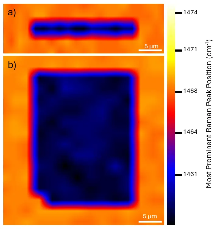
- Patterning. I wrote single spots, lines, and rastered rectangles, then mapped the Raman peak position across each region to check that only the targeted area had changed (map below).
- Kinetics. I tracked the Ag(2) intensity with time-resolved Raman during irradiation at each thickness.
- Devices. I fabricated field-effect transistor test structures on 5 and 10 nm films and measured transport before and after polymerization.
Results
-
Resist-free direct writing. The polymerized regions are sharply confined to where the laser was pointed, with no mask or photoresist. Spots match the ~6 µm laser spot, overlapping spots write ~20 µm lines, and rastering writes ~25 × 30 µm rectangles. Inside a pattern the Ag(2) mode sits within ±2 cm⁻¹ of 1460 cm⁻¹, while the film around it stays at ~1470 cm⁻¹.
-
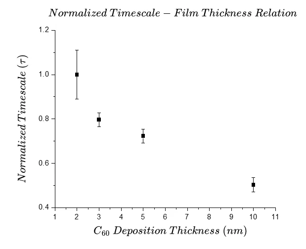
Thicker films react faster. At every thickness the conversion follows a clean single-exponential decay. The fitted timescale falls from τ ≈ 173 s at 2 nm to τ ≈ 84 s at 10 nm, so 10 nm films polymerize about twice as fast. Normalized to the 2 nm film, the timescales for 2 / 3 / 5 / 10 nm are 1.00 / 0.79 / 0.72 / 0.50.
-
Electronics: a useful null. The transistors showed no measurable change in transport between pristine and polymerized films. This marks a boundary on when photopolymerization can be used to “write” electronic properties in this geometry.
Status
I wrote the work up as a manuscript with Y. Wadumethsri and Dr. H. R. Gutiérrez. The project has concluded without a journal submission. The film-growth, patterning, and kinetics results above stand on their own.